Published: September 22, 2026
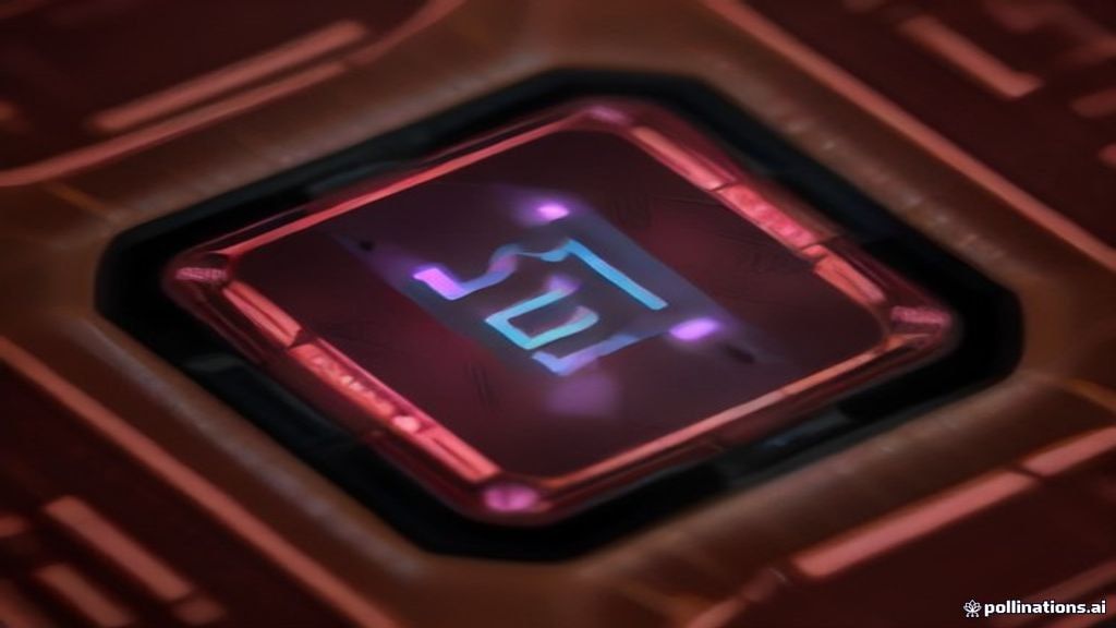
For years, the narrative surrounding artificial intelligence was dominated by a single metric: the sheer scale of model training. We watched as neural networks ballooned from millions of parameters to trillions, driving massive demand for ever-larger GPU clusters. But as we move deeper into 2026, the industry has hit a massive inflection point. The primary engineering bottleneck has officially shifted from training models to running them in production—a phase known as inference.
For electronics engineers, embedded developers, and hardware designers, this shift changes everything. Unlike training, which is a highly parallelizable batch process, inference is real-time, highly latency-sensitive, and increasingly autonomous. With the rise of agentic AI and deep reasoning models (using chain-of-thought processing), systems are running inference loops continuously. This transition is exposing a harsh reality: standard GPU-centric data centers are fundamentally unsuited for the physical constraints of inference workloads. To support this new paradigm, chip architects are completely reinventing how memory and compute interact.
The Silicon Dynamics: Prefill vs. Decode
To understand why traditional hardware fails at inference, we must look at the mathematical execution of a modern transformer-based Large Language Model (LLM). The process is split into two distinct execution phases: prefill and decode.
- Prefill: The model ingests the user's prompt, processing all tokens concurrently. This stage calculates how each token relates to every other token using self-attention. Because this math can be split up and calculated in parallel, highly parallel processors like GPUs excel here. During this phase, the system generates key and value vectors, storing them in memory as the KV cache.
- Decode: This is where the autoregressive bottleneck occurs. The model generates its output sequentially, one single token at a time. To predict the next token, the processor must read the entire model's weights (tens or hundreds of gigabytes) from memory, combine it with the growing KV cache, make a prediction, write the new token back to memory, and repeat.
Because the processor must wait for gigabytes of data to travel across the memory bus just to generate a single token, the compute cores spend most of their time idle. Studies show that state-of-the-art GPUs running open-source LLMs can sit idle up to 80% of the time, starved for memory bandwidth. It is not a compute problem; it is a communication problem.
Reimagining the Memory Interconnect
To bridge this bandwidth gap, semiconductor startups and established players are proposing radically different physical layouts. The standard solution in training hardware is High-Bandwidth Memory (HBM), which stacks DRAM dies around the perimeter of the GPU. However, HBM is expensive and physically limited by the short routing traces required to maintain signal integrity.
Vertical Stack Integration
Companies like d-Matrix are addressing this by building upward. Their Raptor architecture utilizes 3D silicon stacking to place compute logic directly on top of a DRAM die. By shortening the physical distance data must travel from millimeters to micrometers, they drastically lower transmission latency and energy consumption, effectively turning a horizontal board routing problem into a vertical packaging triumph.
Expanding the Memory Shoreline
Taking the opposite approach, Majestic Labs is focusing on expanding the physical distance memory can reside from the processor without sacrificing bandwidth. Instead of relying on the restrictive 2-to-3 millimeter trace limits of HBM, they have engineered a proprietary high-speed copper link coupled with a memory-aggregator chip. This allows their architecture to interface with standard, commodity DRAM up to a meter away, packing up to 128 terabytes of system memory into a single rack—far surpassing the limits of closed HBM systems.
SRAM and the Wafer-Scale Alternative
While DRAM remains the choice for massive capacity, other designers are leveraging SRAM (Static RAM) for its unrivaled speed. While SRAM is significantly less dense and far more expensive than DRAM, it can be etched directly onto the silicon wafer, immediately adjacent to the processing cores.
This is the foundation of the Language Processing Unit (LPU) architecture. By integrating hundreds of megabytes of on-die SRAM directly into the silicon logic, these chips achieve up to seven times the memory bandwidth of traditional GPUs. For decoding, where bandwidth is king, this setup allows for blistering token generation speeds.
Taking this concept to its logical extreme, companies like Cerebras construct wafer-scale engines. By treating an entire silicon wafer as a single giant chip, they can pack tens of gigabytes of SRAM directly onto one piece of silicon. This allows entire models to run completely within on-chip memory, eliminating off-chip bottlenecks and pushing text-generation speeds past 1,000 tokens per second.
Quantization and Alternative Math in Silicon
Hardware engineering does not exist in a vacuum; software co-design is playing a crucial role in mitigating the memory crisis. The most prominent software-hardware optimization is quantization—the process of converting high-precision numbers (like FP16 or FP8) down to lower-precision representations (like 4-bit formats).
By moving to a 4-bit representation (such as the NVFP4 or MXFP4 standards), chip designers can quarter the memory footprint of a model and accelerate compute throughput by up to three times, with negligible loss in reasoning accuracy. This enables hardware to move more parameters per clock cycle, directly speeding up the decode bottleneck.
Other innovators are rethinking computer arithmetic entirely. Startup Tensordyne is developing hardware that runs on a logarithmic number system rather than standard floating-point arithmetic. By representing numbers as exponents, their custom Napier chip can replace complex, power-hungry multiplication circuits with simple addition hardware. This dramatic simplification in silicon layout allows their hardware to deliver massive throughput while operating at a fraction of the thermal design power (TDP) of traditional architectures.
What Lies Ahead for Hardware Developers
We are witnessing the end of the homogenous data center. The era of simply throwing more general-purpose GPUs at AI workloads is giving way to a diverse, heterogeneous systems approach. Modern AI server architectures are increasingly combining different chip classes: using heavy GPU logic for the prefill phase, dedicated memory-centric LPUs for the decode phase, and custom ASICs for hardwired transformer processing.
For the broader electronics community, this revolution highlights a timeless engineering truth: when software paradigms shift, hardware must adapt from the physical silicon up. Whether you are designing low-power edge-AI devices, working with microcontrollers, or building enterprise-scale systems, the focus is clear—processing efficiency is no longer about raw compute cycles; it is entirely about how smartly you move data.
About EDATA SL
EDATA SL shares practical electronics, embedded systems, Arduino, ESP32, Raspberry Pi, IoT, repair guides, DIY projects and technical news for engineers, students and makers.
Original news rewritten with AI for educational purposes.


0 comments:
Post a Comment